


A metal–oxide–semiconductor field-effect transistor, also known as a MOSFET, MOS-FET, or MOS FET, is a type of FET with an insulated gate in which the device’s conductivity is determined by the voltage.
Signal switching and amplifying are done with it. Electronic signals can be amplified or switched with the ability to change conductivity in response to voltage.
In digital and analog circuits, MOSFETs are now even more prevalent than BJTs (bipolar junction transistors).
- Promotion –
The silicon dioxide shapes the Door of the MOSFET. By preventing the direct flow of charges from the gate to the conducting channel, it serves as a means of isolation.
Since hundreds of thousands or even millions of MOSFET transistors can be found in a microprocessor or memory chip, this type of transistor is by far the most common type found in digital circuits.
Complementary pairs of MOS transistors, also known as CMOS logic, can be used to create switching circuits that consume very little power and can be made with either p-type or n-type semiconductors.
Why an MOSFET?
Because their input impedance is nearly infinite, MOSFETs are particularly useful in amplifiers because they can capture almost all of the incoming signal. We choose MOSFET over BJT because it has the main advantage of requiring almost no input current to control the load current.
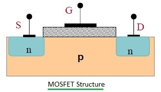
Structure:
“yoastmark It has Source (S), Drain (D), Gate (G), and body (B) terminals. It has four terminals. Frequently connected to the source terminal, the body (B) reduces the number of terminals to three. It works by altering the width of a channel through which electrons or holes carry charge.
The charge transporters enter the channel at the source and exit by means of the channel. The voltage that is applied to an electrode known as Gate, which is situated in between the drain and the source, determines the channel’s width. A very thin layer of metal oxide separates it from the channel.
A metal-insulator-semiconductor field-effect transistor, also known as a MISFET, and a MOSFET are nearly synonymous. IGFET, which stands for insulated-gate field-effect transistor, is another synonym.
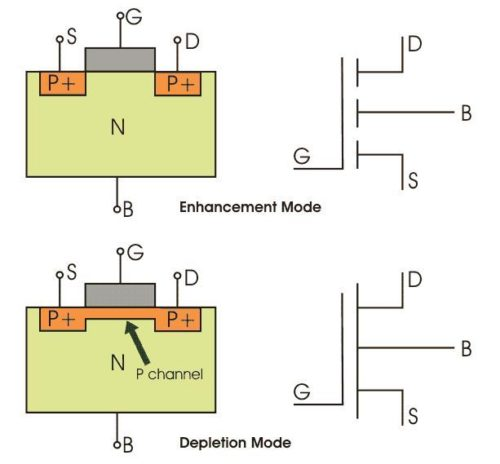
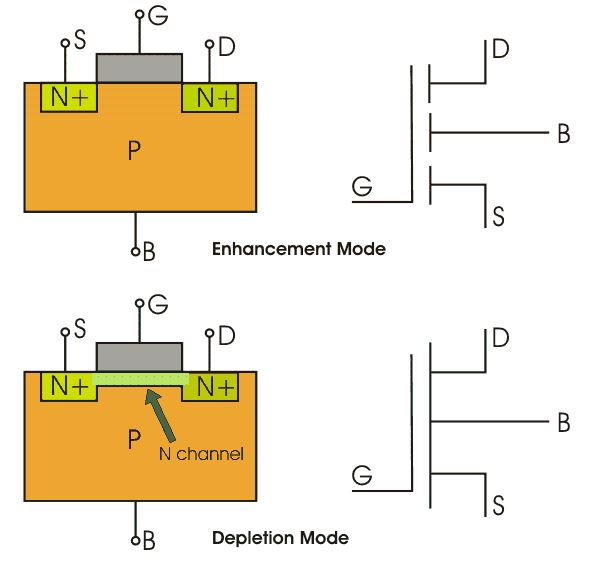
The two main modes of operation of a MOSFET are as follows: 1) Mode of Depletion: To turn the device “OFF,” the transistor needs the Gate-Source voltage (VGS). A “Normally Closed” switch is equivalent to a depletion-mode MOSFET.
2.) Mode of Enhancement: To turn the device “ON,” the transistor requires a Gate-Source voltage (VGS). A “Normally Open” switch is the same as an enhancement-mode MOSFET.
The following is a breakdown of the MOSFET’s working principle:
P-Channel Consumption MOSFET
P-Channel Upgrade MOSFET
N-Channel Consumption MOSFET
N-Channel Upgrade MOSFET
P-Channel MOSFET
P Channel MOSFET Exhaustion and Upgrade Mode
P Channel MOSFET Consumption and Improvement Mode
The channel and source are vigorously doped p+ locale and the substrate is in n-type. Known as a p-channel MOSFET, the flow of positively charged holes causes the current to flow.
The electrons below the oxide layer experience a repulsive force and are pushed downward into the substrate when we apply a negative gate voltage. The bound positive charges that are connected to the donor atoms populate the depletion region.
Additionally, holes from the P+ source and drain region are drawn into the by the negative gate voltage.
P-Channel MOSFET
N-Channel MOSFET
The p-type substrate and heavily doped N+ regions serve as the drain and source. Known as an n-channel MOSFET, the flow of negatively charged electrons causes the current to flow.
Under the oxide layer, the holes experience a repulsive force when the positive gate voltage is applied. As a result, the holes are pushed downwards into the acceptor atoms’ bound negative charges.
An electron reach channel is created because the positive gate voltage also draws electrons into the channel from the N+ source and drain regions.
Operation of the MOSFET
The MOS capacitor is necessary for a MOSFET to function. The MOS capacitor is the principal part of MOS-FET. Between the drain and source terminals is the semiconductor surface beneath the oxide layer. By applying either positive or negative gate voltages, it can be flipped from the p-type to the n-type.
At the point when we apply positive entryway voltage, the openings present under the oxide layer experience a frightful power, and openings are pushed descending with the substrate.
The bound negative charges that are connected to the acceptor atoms populate the depletion region. The electrons enter the channel that has been made. Additionally, the drain regions of the n+ source are drawn into the channel by electrons attracted by the positive voltage.
Now, the electrons in the channel are controlled by the gate voltage if a voltage is applied between the drain and source. Current flows freely between the drain and source. Under the oxide layer, a hole channel will form if we apply a negative voltage.
Applications
Amplifiers for DC Motor Regulation, Chopper Amplifier Construction, Switching, and Amplifying Signals You can also check out the slideshow presentation below:
Credit: The MOSFET (Metal Oxide Semiconductor Fet) from stooty s This section of the article concludes our discussion of the MOSFET’s fundamentals.
If you have any doubts or questions, you can ask them in the comment section below or use our Forum to talk to the community of engineers and electronics hobbyists.