


The earliest form of FET is the Junction Field Effect transistor (JFET). Between the drain terminals and the sources, the current moves through an active channel. The JFET’s electric current flow between the source and drain is controlled by the voltage applied between the gate and source. The electric current is completely turned off when a reverse bias voltage is applied to the gate terminal, straining the channel. JFETs are referred to as “normally on” devices for this reason. There are P-channel and N-channel JFET transistors available.
N-Channel JFET
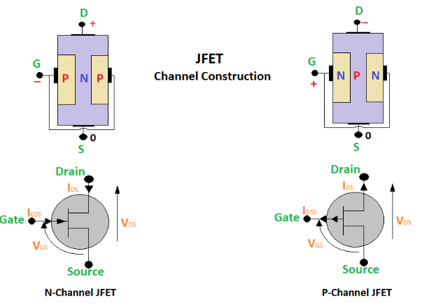
The channel in the N-channel JFET is an N-type semiconductor because it is doped with donor impurities. As a result, electrons flow in a negative direction through the channel. Hence, the N-channel JFET name. Doped at opposite sides, these are two P-type substrates in the middle. These heavily doped P-type regions and the N-type channel in between create two PN junctions. The drain (D) and source (S) leads are connected to either end of the N-type channel, while the gate (G) lead is internally connected to both P-type terminals.
How does it work?
The channel opens up to allow electrons to flow freely when the gate terminal is depleted of voltage. As a result, the source terminal receives the most current. The internal resistance of the channel and the potential difference between the source and drain terminals determine the amount of current flow.
However, the P-N junction becomes reverse biased when a negative voltage is applied to the gate terminal in relation to the source terminal. An exhaustion locale is made in the channel that makes the channel smaller, expanding the channel obstruction between the source and channel, and the ongoing stream turns out to be less.
P-Channel JFET
Similar to the P-channel JFET, the channel is a P-type semiconductor because it is doped with acceptor impurities. As a result, holes represent positive current flow through the channel. Hence, the P-channel JFET name. N-type substrates heavily dope the channel’s opposite side. The gate terminal is formed by joining the N-type regions on both sides, as in an N-channel JFET. The terminals for the source and drain are taken from the two other sides of the channel.
An N-channel JFET’s operating principle is also comparable. The only difference is that to turn it off, you need to connect a positive gate to the source voltage. In any case, N-channel JFET has a more prominent current conductivity because of lower channel opposition than their identical P-channel types, since electrons have higher versatility through a guide contrasted with openings. This makes the N-channel JFET more effective than their P-channel partners.
How does it work?
A DC supply is used here to bias a JFET, which will control the JFET’s VGS. We have some control over the applied voltage across the Channel and Source terminal by fluctuating the VGS. The JFET’s I-V characteristics curve can be plotted from there.